400-888-2483
 我的账户
我的账户


-
可编程晶振空白片FP >
-
MHz有源晶振 >
-
差分晶振 >
-
汽车级晶振 >
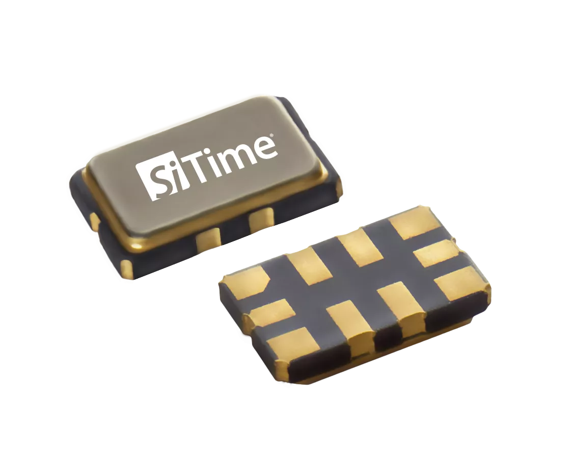
差分
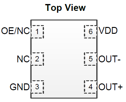
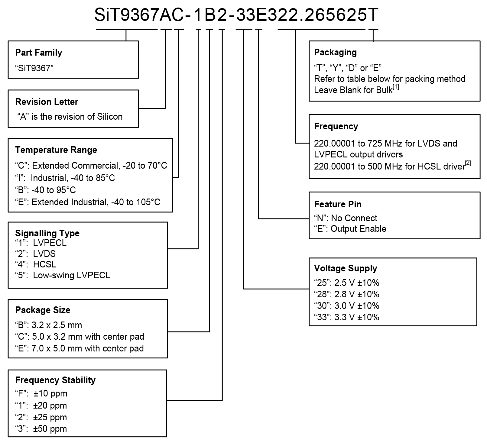
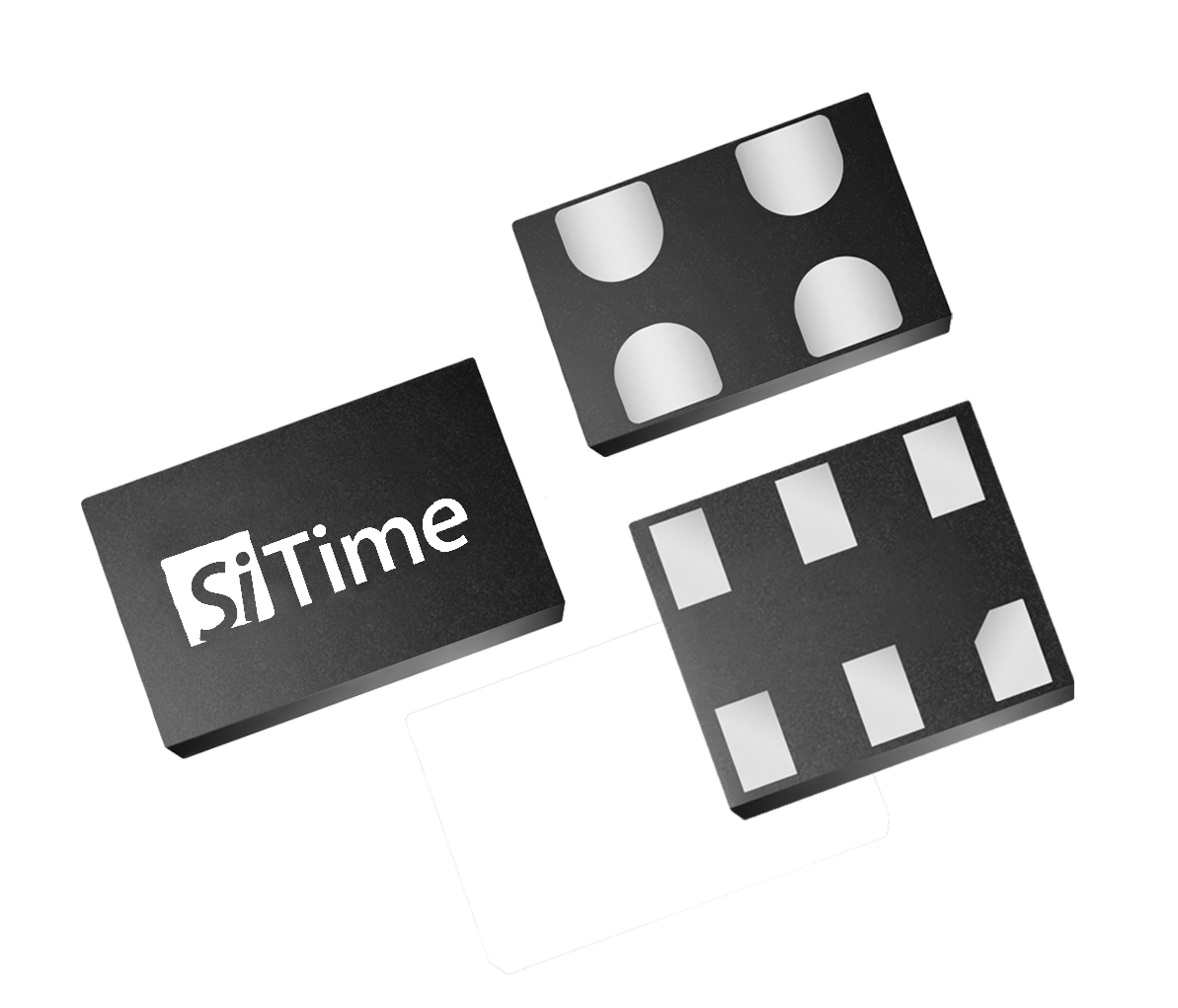
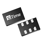
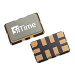
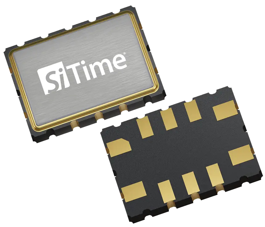
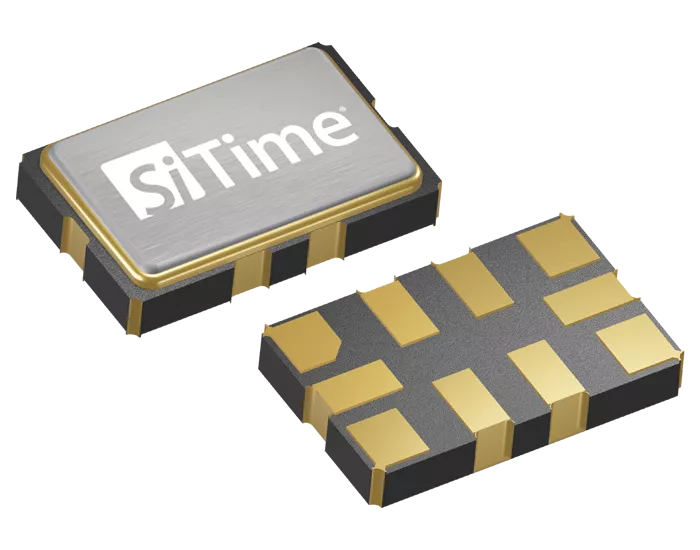
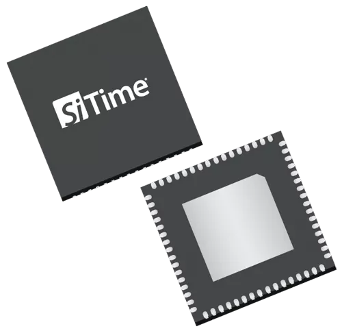
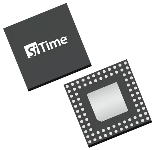
SiT93861-220MHz任意频率,AEC-Q100,汽车级差分晶振LVPECL/LVDS/HCSL
SiT9386
1-220MHz任意频率,AEC-Q100,汽车级差分晶振LVPECL/LVDS/HCSLSiT9387-40~105℃,220-725MHz任意频率,LVDS/LVPECL/HCSL差分信号
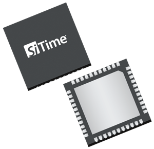
SiT9387
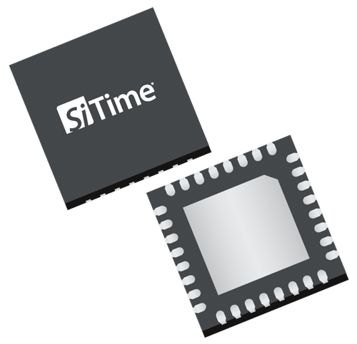
-40~105℃,220-725MHz任意频率,LVDS/LVPECL/HCSL差分信号SiT9396-40~125℃,1-220MHz任意频率,LVDS/LVPECL/HCSL差分信号
SiT9396
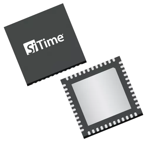
-40~125℃,1-220MHz任意频率,LVDS/LVPECL/HCSL差分信号SiT9397-40~125℃,220-920MHz任意频率,LVDS/LVPECL/HCSL差分信号
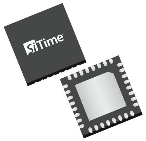
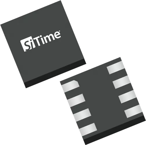
SiT9397
-40~125℃,220-920MHz任意频率,LVDS/LVPECL/HCSL差分信号 -
抗冲击宽温晶振 >
-
压控晶振VCXO >
-
高精度温补晶振TCXO >
-
恒温晶振OCXO >
-
32.768KHz >
-
扩频晶振SSXO >
-
I2C/SPI / 数控晶振 >
-
网络同步 / 去抖时钟 >
-
时钟发生器 >
-
时钟缓冲器(buffers) >